
AI-Powered 12-Inch Wafer Inspection: How Advanced Microscopy Is Transforming Semiconductor Manufacturing
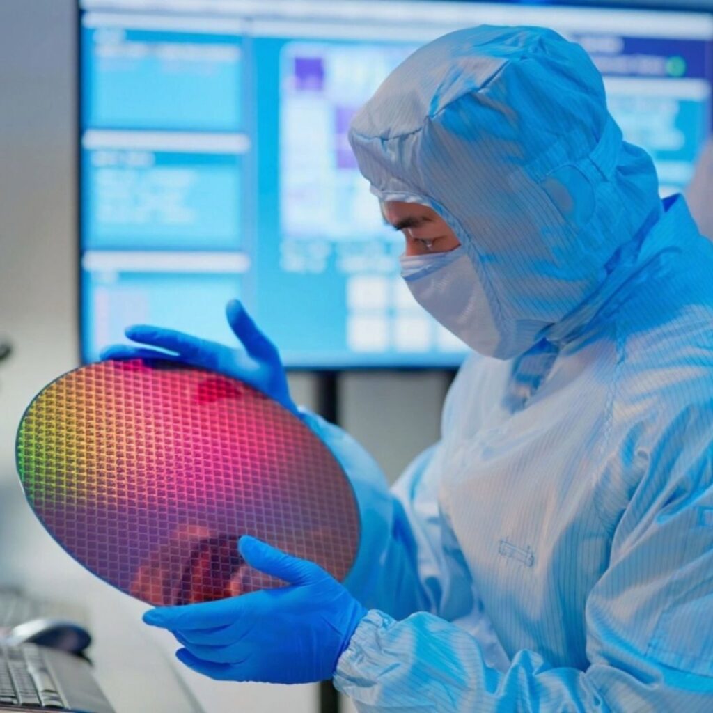
The semiconductor industry is evolving rapidly, with manufacturers constantly striving for higher yields, smaller nodes, and faster production cycles. But with increasing wafer sizes — especially 12-inch (300mm) wafers — microscopic defects can cost millions of dollars in losses if not detected early.
Traditional wafer inspection techniques often fail to meet modern manufacturing demands. That’s where AI-powered wafer inspection systems integrated with advanced microscopy are transforming the industry by delivering nanometer-level defect detection, real-time classification, and predictive analytics.
The Growing Challenge of 12-Inch Wafer Inspection
As chip designs become smaller, denser, and more complex, quality control in 300mm wafer manufacturing faces multiple challenges:
⚠️ Microscopic Defects Impact Yield: Even a single particle or scratch can render an entire wafer unusable.
⚡ Increasing Production Volumes: Manual inspection slows down high-volume manufacturing.
🔍 Traditional Optical Systems Are Limited: Standard inspection tools can’t always detect sub-micron defects.
📉 High Costs of Errors: Missed defects lead to rework, production delays, and financial losses.
This calls for a next-generation wafer inspection approach that combines AI + microscopy for unmatched accuracy and efficiency.
AI + Microscopy: A Smarter Approach to Wafer Inspection
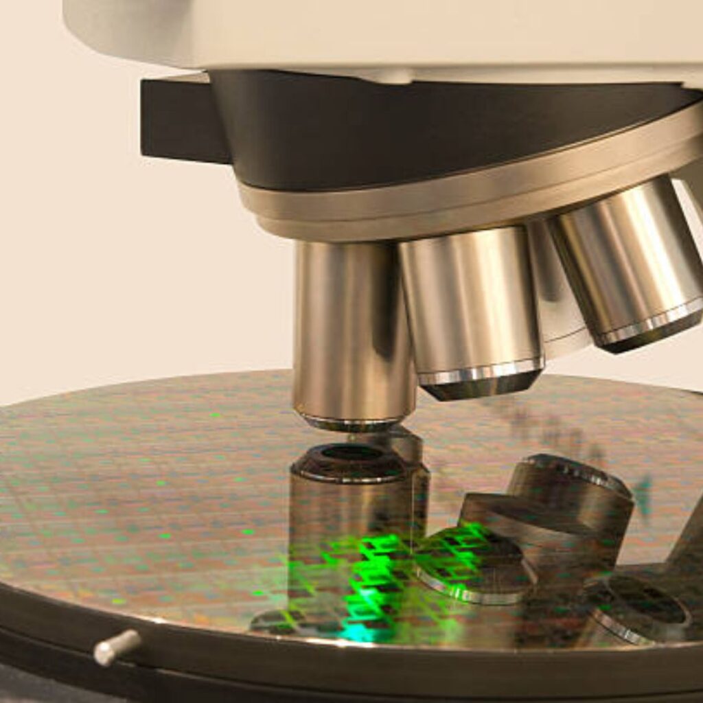
Our AI-powered 12-inch wafer inspection solution leverages high-resolution microscopy and machine learning to automate, accelerate, and improve defect detection.
Key Innovations & Features
1. Nanometer-Level Defect Detection
High-resolution microscopy identifies defects as small as 50nm.
Ensures no hidden particles, scratches, or cracks escape detection.
2. AI-Driven Real-Time Classification
Intelligent algorithms classify thousands of defects instantly.
Reduces manual inspection time by up to 40% while increasing accuracy.
3. Faster Throughput & Yield Optimization
Automates repetitive inspection tasks.
Reduces inspection cycle times and accelerates time-to-market.
4. Scalable for R&D and Mass Production
Suitable for both semiconductor research labs and high-volume fabs.
Fully customizable for different wafer types and production needs.

Benefits for Semiconductor Manufacturers
Adopting AI + microscopy wafer inspection delivers measurable improvements across the production cycle:
| Benefit | Traditional Inspection | AI + Microscopy |
|---|---|---|
| Defect Detection Accuracy | Limited to visible defects | Nanometer-level precision |
| Inspection Speed | Manual, time-consuming | 40% faster automated process |
| Defect Classification | Subjective, prone to errors | AI-driven, 99% accuracy |
| Yield Improvement | Slower defect correction | Higher wafer yield, reduced scrap |
Industries & Applications
Our solution is ideal for:
🏭 Semiconductor Fabs – Ensure zero-defect manufacturing
🔬 R&D Laboratories – Accelerate process innovation
🏢 OEM Semiconductor Equipment Manufacturers – Integrate AI inspection tools
🧪 Testing & Quality Control Labs – Automate inspection workflows
Why Choose Our AI-Powered 12-Inch Wafer Inspection System
🚀 40% faster inspection turnaround
🔍 Detects defects as small as 50nm
🤖 AI-driven real-time defect classification
📊 Integrated predictive analytics for process optimization
🌐 Scalable for both lab testing and high-volume fabs
By combining AI intelligence with microscopic precision, we empower semiconductor manufacturers to achieve better yields, lower costs, and higher production efficiency.
The Future of Wafer Inspection
As the industry moves toward 2nm and beyond, defect detection complexity will increase exponentially. Manufacturers who adopt AI + microscopy-based inspection today will have a significant advantage in achieving high yields and superior process control.
The future of semiconductor quality control lies in automation, real-time analytics, and intelligent defect mapping — and this technology delivers all three.