
About Our
Company
HEXON Instruments is established to provide smart solutions for the customers needs. Our values comprise of Passion, Trust, Team spirit, Dynamism, Integrity and Delight Customers. Our sole objective is to give the best user experience to all our customers with our best after sales support.
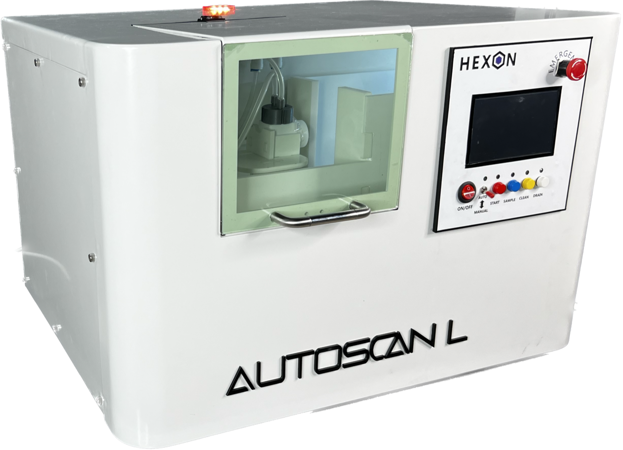
Our Manufacturing Facilities
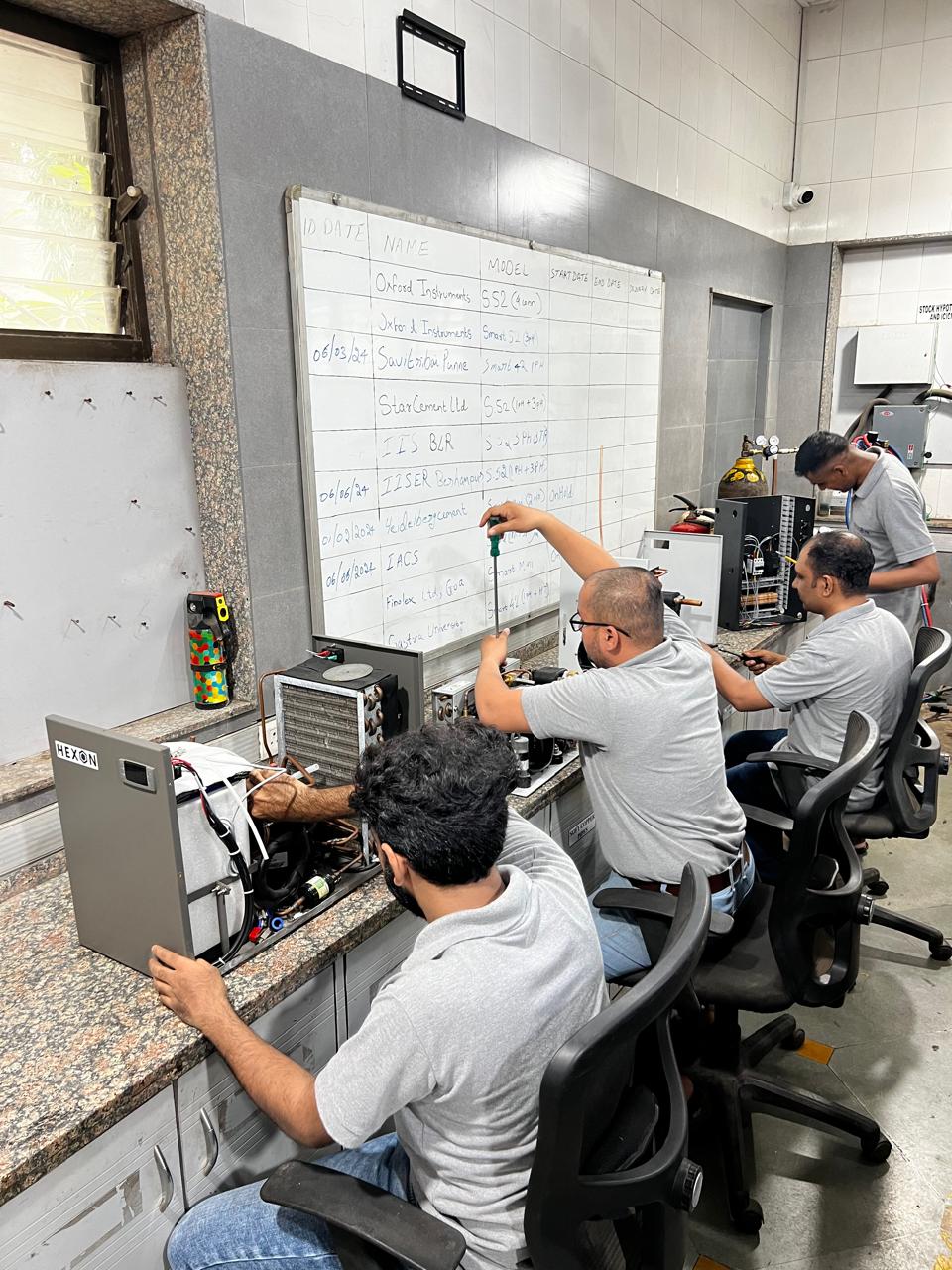
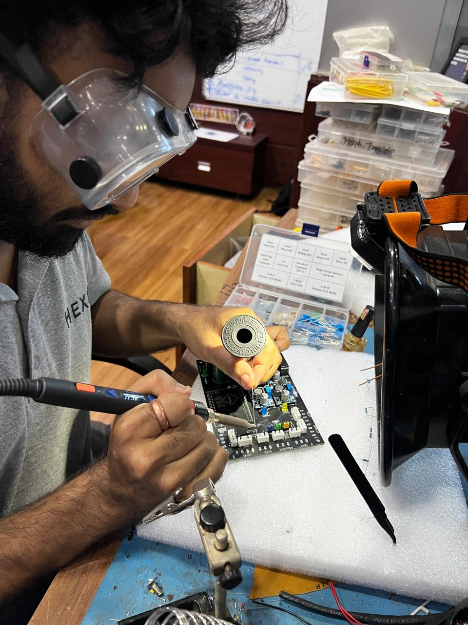
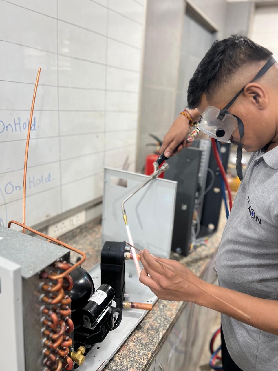
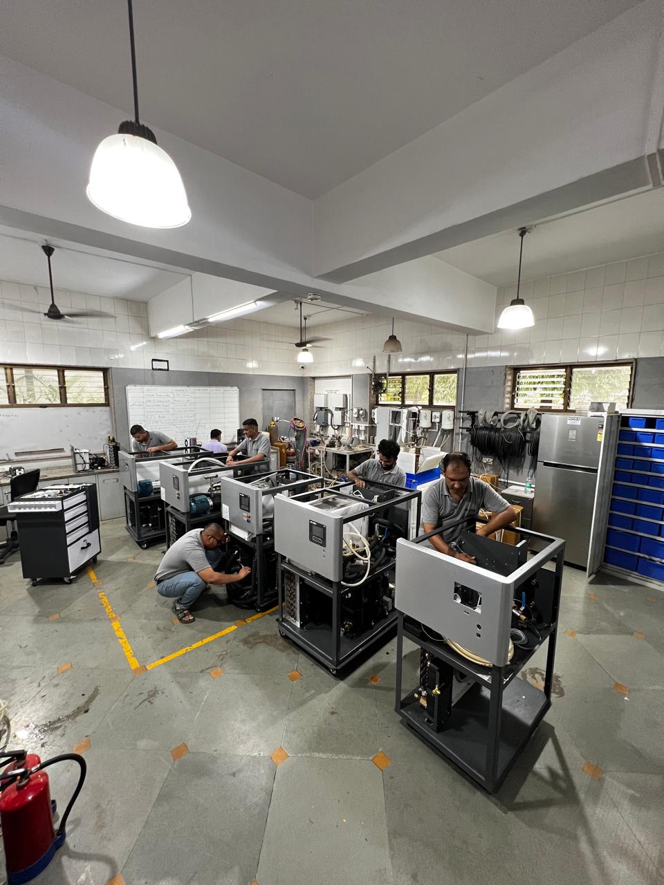
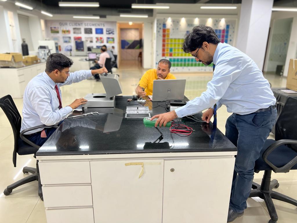
At Hexon Instruments, we take immense pride in our state-of-the-art manufacturing facilities, designed to uphold our commitment to quality, innovation, and efficiency. Our facilities are equipped with the latest technology and infrastructure to ensure we meet the highest standards of production and safety.
Why Choose Us
- Make in India
- Trust
- Global Standard
- Quality
- 24*7 Support
Let's Get In Touch!
Industry We Serve

Education Institutes

Top Labs

Pharma Companies

Food Research

Metal

Mining

Environmental

Petrochemical
Industry We Serve
Education Institute
Top labs
Pharma companies
Food research
Metal
Mining
Environmental
Petrochemical
Latest News & Blog


Our Prestigious Clients
















Frequently Asked Question
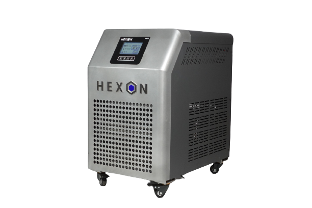
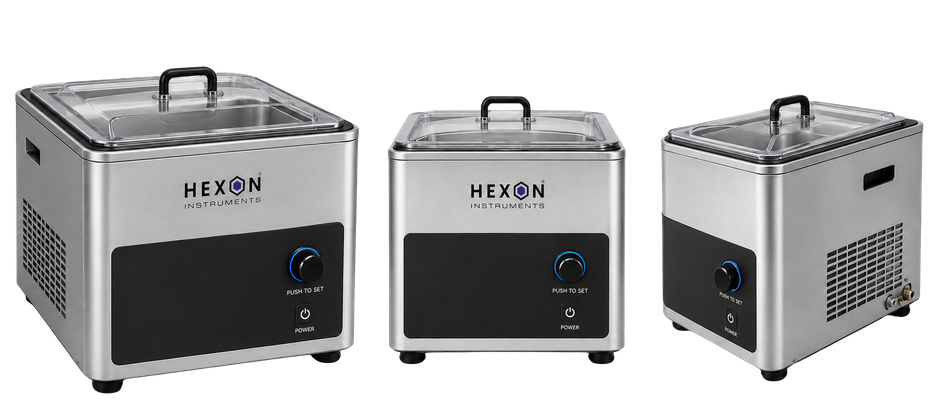
A water recirculating chiller is a closed-loop cooling system that circulates chilled water (or water-glycol mixture) through equipment to remove heat and maintain a stable temperature.
A hot stage is a temperature-controlled sample holder that allows you to heat (and sometimes cool) a specimen while observing it under a microscope. It enables real-time study of how materials change with temperature.
Our standard systems accommodate 250×250mm scanning areas suitable for most applications. For larger substrates or specialized formats, we offer custom motorized stage configurations up to 500×500mm travel range. Our engineering team works directly with customers to design optimal scanning solutions for unique production requirements, including multi-panel inspection and custom fixture integration.
Hexon provides comprehensive 24/7 technical support via phone, email, and remote assistance. All systems include a standard 12-month warranty covering parts and labor. We offer annual maintenance contracts (AMC) with scheduled preventive maintenance visits, optical calibration verification, and priority spare parts supply. Our service engineers are based across major industrial hubs in India, ensuring rapid on-site response within 24-48 hours for critical issues.
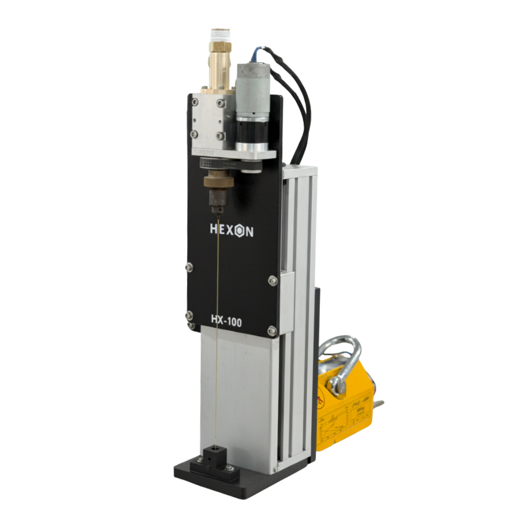
Single pulse EDM produces just one spark discharge instead of a continuous series of sparks (as in conventional EDM). This allows precise observation of:
Material removal mechanism
Crater formation
Heat-affected zone
Indian manufacturing has earned global trust when quality and documentation meet expectations. We design our online analyzers with export requirements in mind from the beginning.
As a growing online analyzer exporter from India, we support customers and partners who install systems across different regions and regulatory environments.
International Standards & Quality Assurance
Exported analyzers are tested against performance parameters expected by international buyers. Electrical safety, enclosure integrity, and measurement stability are verified before dispatch.
Documentation is prepared clearly to support customs clearance, installation, and future servicing.
Clients abroad often work across time zones. Clear manuals and responsive technical communication reduce delays during commissioning. This practical approach helps build long-term export relationships rather than one-time shipments.
Today’s digital economy depends entirely on advanced semiconductor products, where inspection processes throughout manufacturing become essential to ensure high quality and reliability of final products. These inspection challenges grow increasingly complex and costly at each production step, as defect tolerance decreases due to smaller features, design complexities, and wafer-level integration requirements.
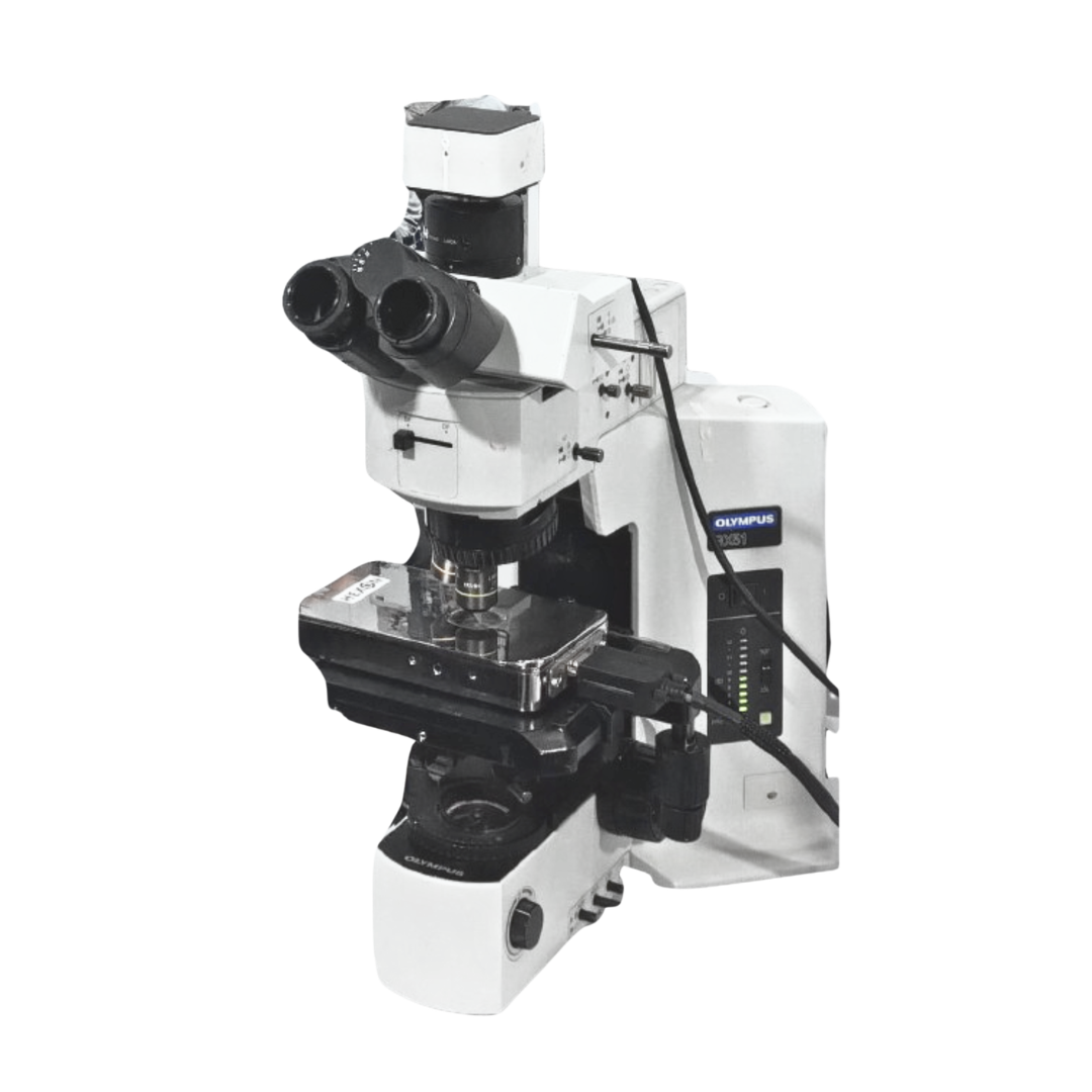
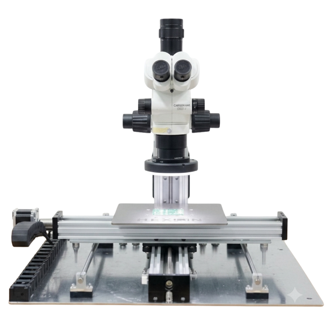
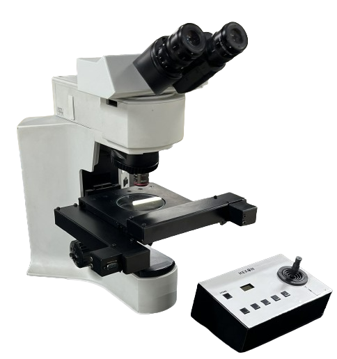
Hexon Instruments has launched a revolutionary automated optical inspection system (AOI) specifically designed to address these manufacturing challenges. Our AOI integrates a high-resolution microscope with a precision motorized XY stage for automated scanning of semiconductor wafers, electronic circuits (PCBs), and solar cells to detect defects like cracks, voids, particles, line breaks, shorts, and soldering issues.
Silicon Wafer Defect Detection Capabilities
Our AOI system handles semiconductor wafers up to 300mm diameter with vibration-free operation, high accuracy, and exceptional repeatability. The system is designed on a sturdy platform base that supports high-resolution cameras and microscopes whilst maintaining stable imaging conditions throughout extended inspection cycles.
Common defects detected across semiconductor manufacturing include:
Line breaks or shorts in circuit patterns that compromise electrical connectivity
Particle contamination on wafer surfaces that can cause device failures
Manufacturing anomalies including alignment errors, etch defects, and deposition irregularities
Shunts creating unwanted conductive paths between circuit elements
The system maximises defect sensitivity whilst maintaining throughput necessary for complete wafer coverage in production environments. This balance between sensitivity and speed makes our AOI solution practical for high-volume manufacturing whilst maintaining the detection accuracy required for quality assurance.
Key Features of Our AOI Platform
Our automated optical inspection system incorporates several advanced features that distinguish it from basic inspection equipment. The motorized stage enables precise, programmable scanning across large areas including full wafers up to 300mm without manual repositioning, supporting high-throughput inspection requirements in manufacturing environments.
The microscope integration uses high-resolution optics with auto-focus capabilities and multi-mode lighting including brightfield and darkfield illumination for clear imaging of surface defects under various optical conditions. This flexibility ensures that subtle defects remain detectable regardless of surface characteristics or material properties.
Automation software includes defect detection algorithms, AI-based classification systems, and automated reporting functions for identifying anomalies in real-time with fail and pass buzzer feedback. The 300 × 300 mm stage provides vibration-free operation with exceptional accuracy and repeatability, making the system ideal for automated micro-inspection applications in demanding manufacturing environments.
Printed Circuit Board and Solar Cell Analysis
Beyond semiconductor applications, our AOI systems excel at printed circuit board inspection, detecting open circuits (broken or incomplete copper traces) and short circuits (copper bridging between adjacent traces) that could cause product failures. The multi-mode lighting capabilities ensure clear imaging of surface defects across different substrate materials and finish types.
For solar cell manufacturing, the system identifies finger interruption (broken metal grid lines) and shunts (unwanted conductive paths) that reduce cell efficiency and power output. The programmable scanning capabilities enable inspection patterns optimised for solar cell geometries, supporting quality control requirements throughout photovoltaic manufacturing processes.