
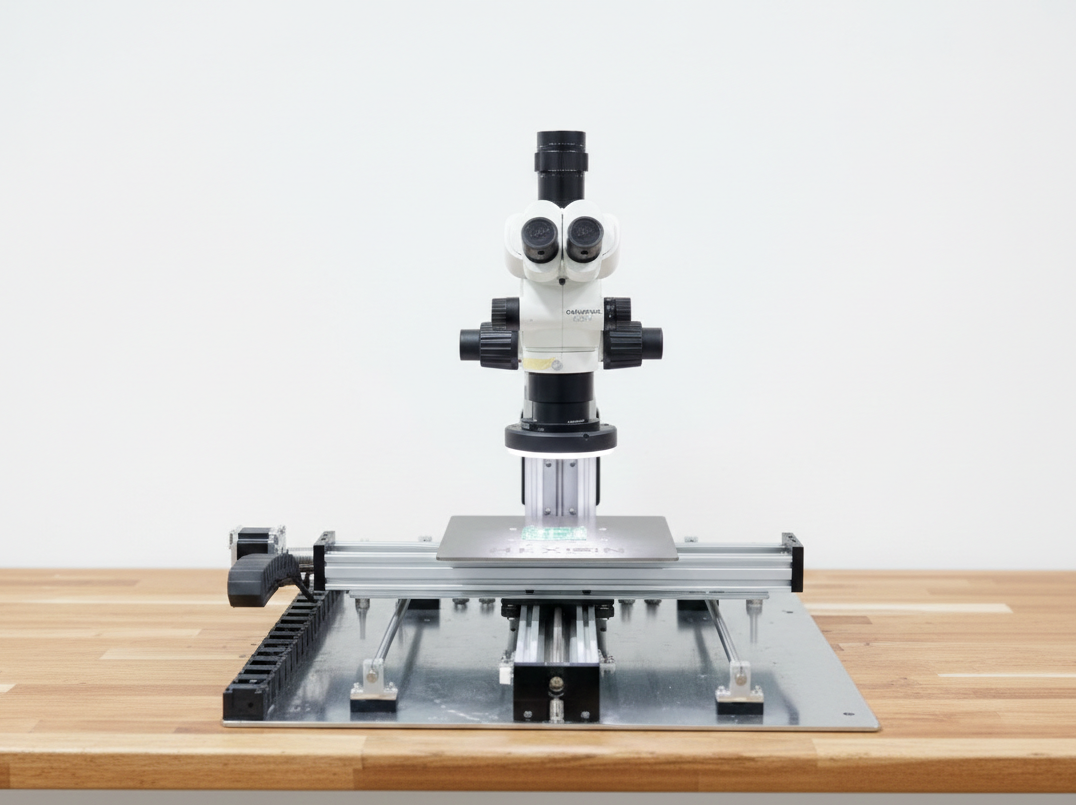
The Hexon AOI System integrates a high-resolution microscope with a precision motorized XY stage, enabling automated scanning of semiconductor wafers, PCBs, and microelectronic components for rapid, repeatable defect detection including cracks, voids, particles, and soldering defects with micron-level accuracy.
Quality control in semiconductor and electronics manufacturing demands precision that human inspection cannot consistently deliver. Manual defect detection introduces variability, operator fatigue, and throughput limitations that compromise yield and increase costs.
At Hexon Instruments, we recognise these challenges facing India’s growing semiconductor ecosystem and electronics manufacturing sector. Our newly launched Automated Optical Inspection (AOI) System addresses these critical needs through intelligent automation, advanced optical performance, and AI-driven analytics that transform quality workflows.
System Architecture and Core Capabilities
The Hexon AOI platform combines advanced imaging technology with programmable motion control to deliver consistent inspection outcomes across large sample areas. Our system architecture eliminates operator dependency whilst maintaining the flexibility required for diverse manufacturing environments.
Integrated High-Resolution Optical System
Our AOI system features advanced microscopy with magnification ranging from 5x to 100x or higher, accommodating multi-scale inspection requirements from macro-level component placement verification to micro-level solder joint analysis.
Auto-focus functionality maintains consistent image clarity across samples with varying surface topologies, preventing the focus drift that compromises defect detection in conventional systems. Multi-mode illumination including brightfield and darkfield capabilities ensures optimal contrast for detecting subtle defects across different substrate materials and surface finishes.
Precision Motorized XY Stage Performance
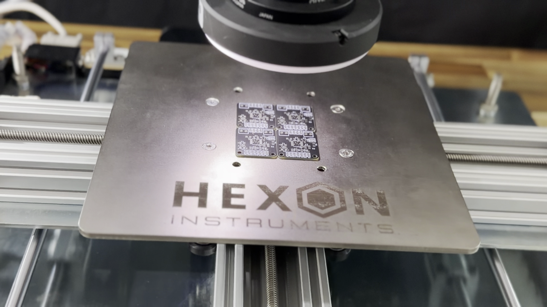
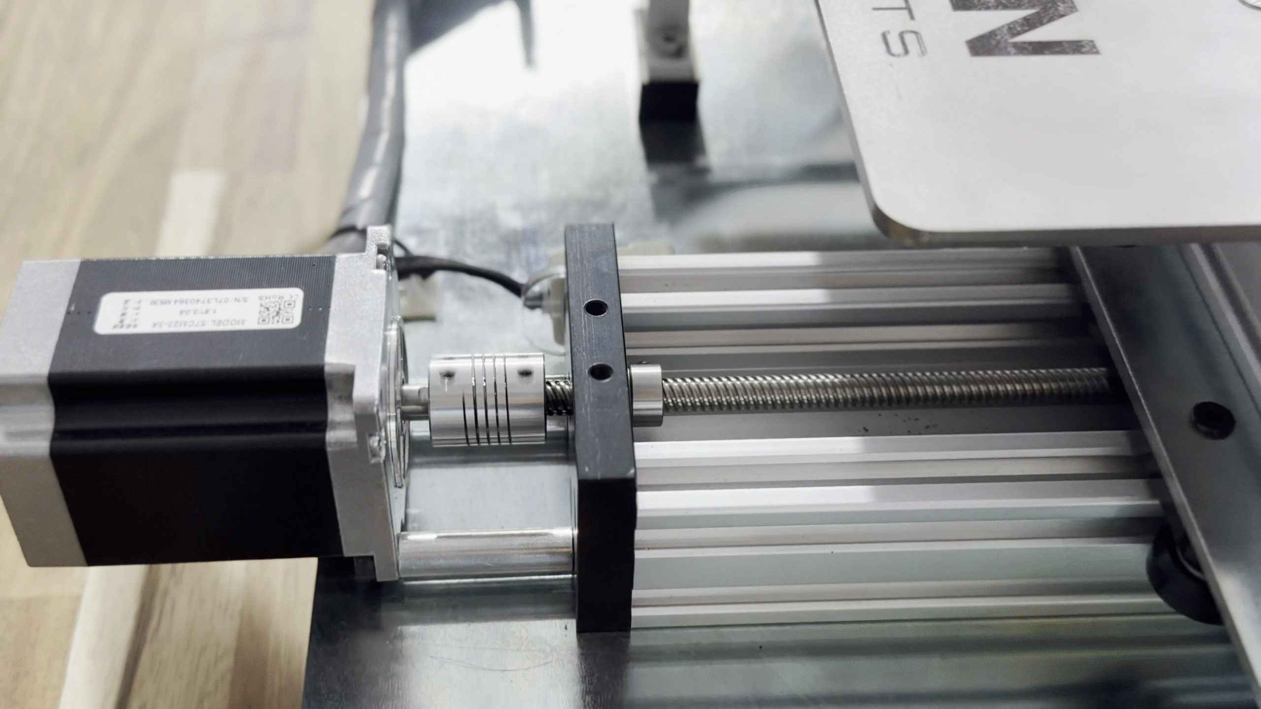
At the heart of our AOI system lies a precision motorized stage with 300x300mm travel range, supporting automated inspection of semiconductor wafers up to 300mm diameter and large PCB panels without repositioning. The stage delivers positioning repeatability better than 2 micrometres with vibration-free operation that prevents image degradation during scanning.
Linear encoder feedback systems enable resolution down to 50 nanometres in premium configurations, whilst cost-effective stepper motor variants achieve 0.15 to 1 micrometre resolution suitable for most electronics inspection applications.
Speed characteristics adapt to inspection requirements: fine controlled motion below 1mm/s for critical defect scanning, and high-performance scanning up to 750mm/s for rapid large-area coverage. The platform supports centered loads of 35 to 100 Newtons, accommodating substantial optical assemblies and sample fixtures without compromising motion accuracy.
Technical Specifications
Our Automated Optical Inspection system delivers industrial-grade performance through precision-engineered components and intelligent control systems designed for demanding manufacturing environments.
Stage Performance Specifications:
- Travel Range: 250x250mm standard, scalable to 300x300mm for large wafer and PCB panel inspection
- Positioning Accuracy: ±5 µm to ±10 µm depending on configuration
- Repeatability: <0.5 µm to ~2 µm across full travel range
- Resolution: 50 nm with linear encoders, 0.15-1 µm with stepper systems
- Speed Range: Fine motion <1 mm/s, high-speed scanning up to 750 mm/s
- Load Capacity: 35-100 N centered load (3-10 kg)
- Motion Control: Crossed roller bearings for ultra-smooth vibration-free operation
Optical System Specifications:
- Magnification Range: 5x to 100x or higher for multi-scale inspection
- Auto-Focus: Integrated functionality for consistent imaging clarity
- Illumination: Multi-mode brightfield and darkfield configurations
- Wafer Support: 4-inch, 6-inch, and 8-inch formats
- Image Quality: Enhanced micro-defect visualization capabilities
Software and Automation Features:
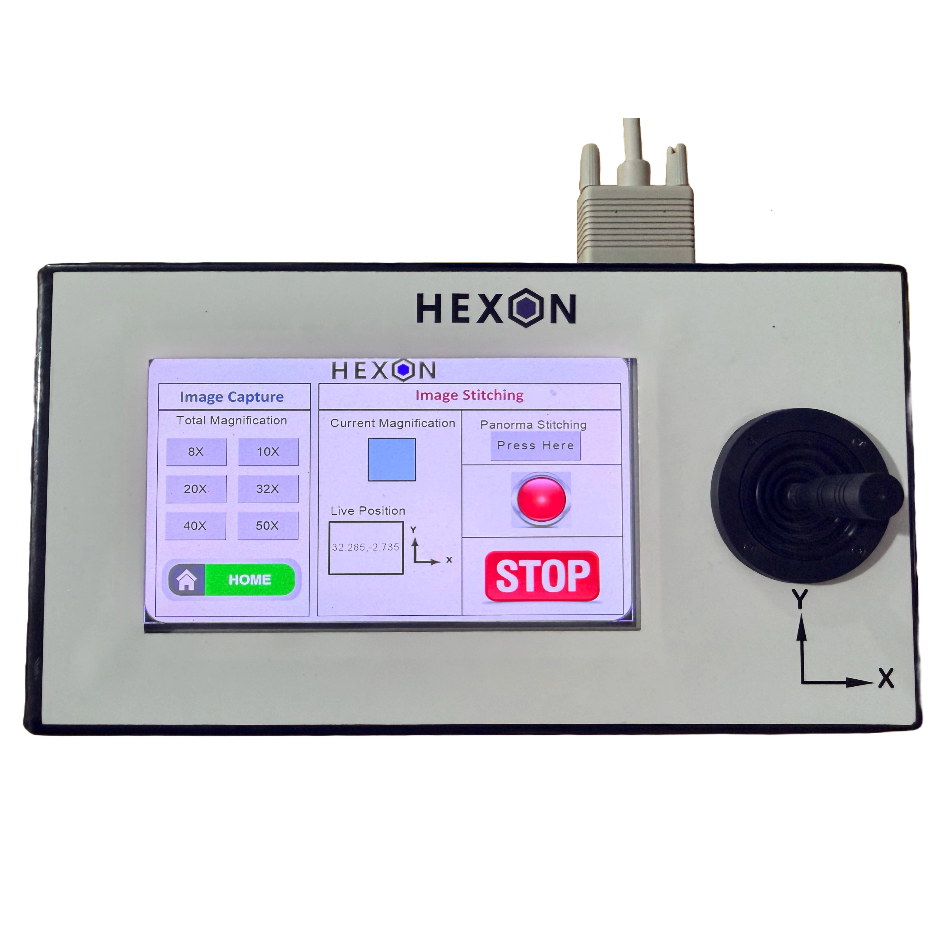
- Connectivity: USB, RS-232, and Ethernet interfaces
- Integration: Compatible with Hexon Microscopy Automation Software
- Scanning: Programmable automated inspection workflows
- Image Processing: Real-time defect detection algorithms with machine learning
- Classification: Pass/Fail determination with audible buzzer alerts
- Data Management: Inspection logging, reporting, and traceability functions
- Image Stitching: Large-area panoramic reconstruction
Environmental and Operational Parameters:
- Operating Temperature: 0°C to 50°C
- Mechanical Stability: Industrial-grade platform construction
- Drive Options: Linear motors with encoders (premium) or stepper motors with rotary encoders (cost-effective)
Key System Features
1. Intelligent Automation and AI-Driven Analytics: Real-time defect detection algorithms powered by machine learning analyse images during scanning, identifying anomalies through pattern recognition and classification techniques that exceed human visual inspection capabilities. Our automation software generates programmable scanning workflows that execute complex inspection sequences without operator intervention.
2. Comprehensive Defect Detection Capabilities: The system identifies critical manufacturing defects including line breaks, shorts, particle contamination, shunts, solder joint irregularities, component misalignment, and copper trace defects. Pattern recognition algorithms distinguish between acceptable process variations and genuine quality issues, reducing false rejection rates whilst maintaining stringent defect capture requirements.
3. Traceable Quality Workflows: Inspection data logging creates comprehensive quality records with defect coordinates, classifications, timestamps, and sample identification. This traceability supports ISO certification requirements, regulatory compliance, and continuous improvement initiatives where defect trend analysis guides process optimization.
Industry Applications Across Manufacturing Sectors
The Hexon AOI system serves diverse manufacturing environments where automated defect detection directly impacts product quality, yield optimization, and regulatory compliance. Our platform addresses critical inspection challenges across semiconductor fabrication, electronics assembly, and precision manufacturing operations.
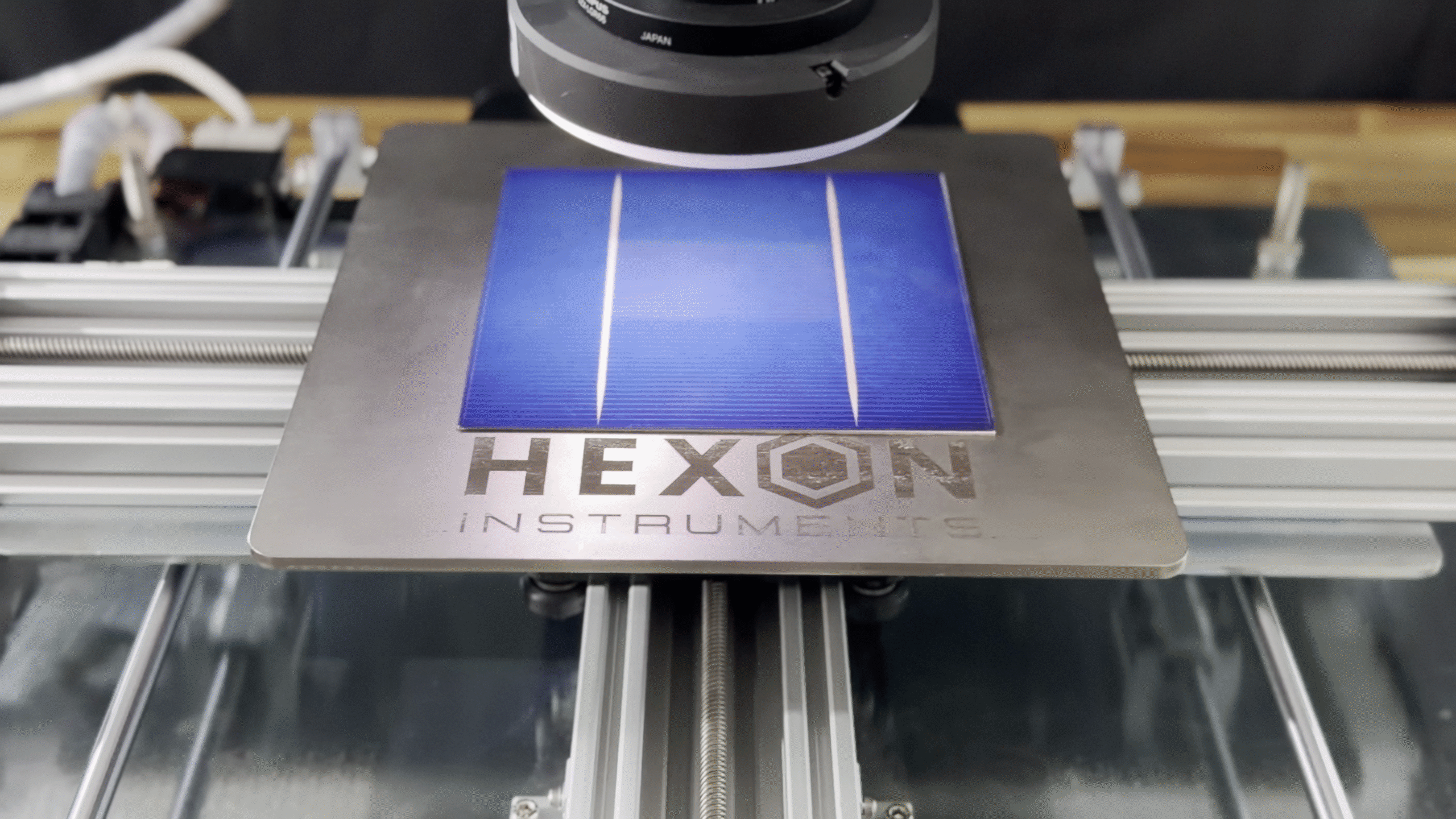
Semiconductor Wafer Inspection
Silicon wafer manufacturing demands defect detection at nanometre scales where particle contamination, line breaks, shorts, and shunts compromise device yields.
Our AOI system supports 4-inch, 6-inch, and 8-inch wafer formats with automated scanning protocols that map defect distributions across entire wafer surfaces. This capability proves essential during process development and qualification where defect density measurements validate manufacturing capability.
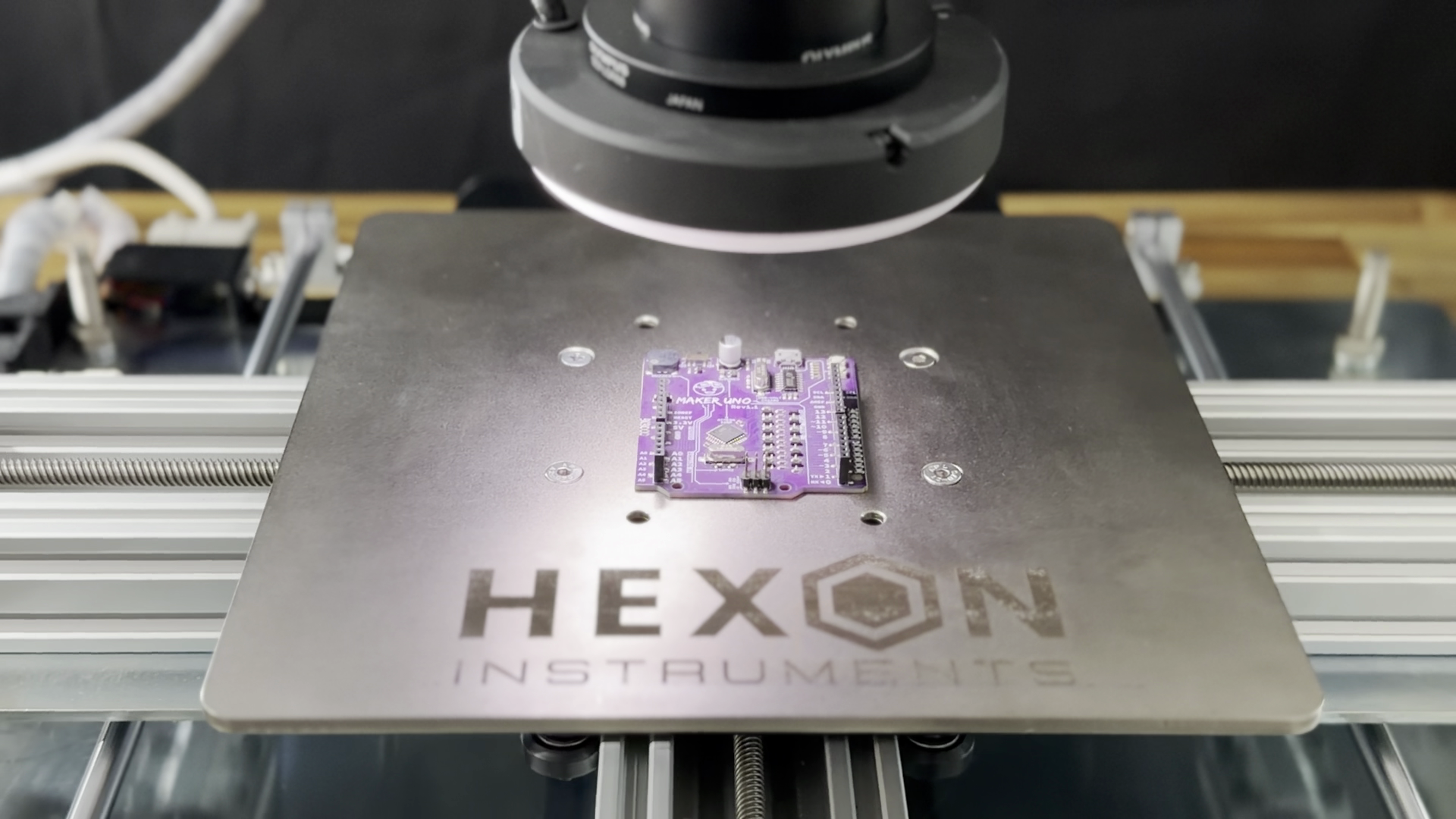
Electronics and PCB Manufacturing Quality Control
Printed circuit board assembly introduces defects including insufficient solder, bridging between adjacent pads, component misalignment, and copper trace defects.
Automated solder joint inspection verifies connection integrity faster and more consistently than manual optical inspection, whilst component placement verification confirms correct part positioning before reflow. Track and pad defect detection identifies opens and shorts that would cause circuit failures, protecting against costly field returns.
Advanced Manufacturing and MEMS Inspection
Micro-electromechanical systems, sensors, and precision assemblies require inspection capabilities that reveal structural defects at microscopic scales.
Our platform supports material defect characterisation during R&D, quality benchmarking against specifications, and process development validation where inspection feedback guides manufacturing optimisation.
Modular Architecture for Factory Automation
The Hexon AOI platform features modular design architecture enabling scalability toward complete factory automation as manufacturing volumes grow. This forward-looking approach protects initial equipment investments whilst supporting graduated automation implementation aligned with production scale and capital availability.
Future automation upgrade pathways include:
- Robotic Loading Arms: Automatic PCB and wafer pickup and placement eliminating manual handling
- Automated Bin Sorting: Pass/Fail segregation without operator intervention
- Conveyor Integration: Inline production workflows with continuous inspection capability
- Barcode/QR Code Readers: Batch-level tracking and automated product identification
Supporting India's Semiconductor Vision
As India advances toward semiconductor self-reliance under the Make in India initiative, domestic manufacturing of precision inspection equipment becomes strategically important. Hexon Instruments, based in Navi Mumbai’s MIDC Industrial Area, delivers international-grade AOI technology at accessible costs, eliminating import dependencies and currency fluctuations whilst supporting local technical expertise development.
Our commitment extends beyond equipment supply to comprehensive application support, custom automation development, and long-term partnership that grows with your manufacturing capabilities.
Consult with Hexon Experts
Manufacturing teams seeking to enhance defect detection accuracy, reduce inspection costs, and implement traceable quality workflows can contact Hexon Instruments for tailored automation consultation. Our technical team provides detailed application analysis, system configuration recommendations, and complete integration support.
Email us at info@hexoninstruments.com or call +918657448273 to discuss how our AOI platform can transform your quality control operations.