
Automated Optical Inspection for Reliable Defect Detection
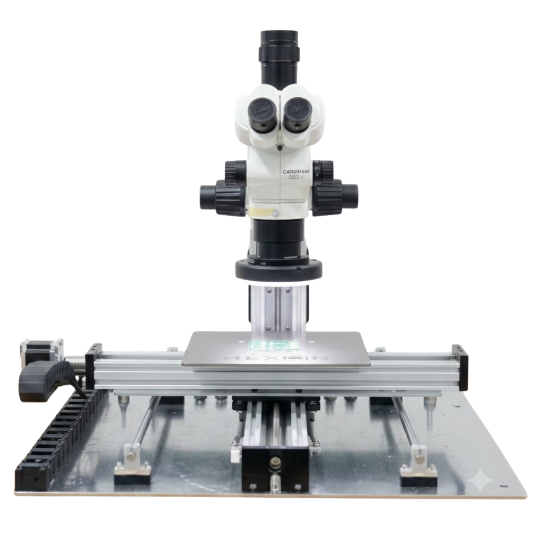
Engineered for Critical Quality Control
From semiconductor wafer inspection to advanced PCB manufacturing, our Automated Optical Inspection (AOI) system delivers precision across diverse applications.
Semiconductor Wafer Inspection
Detect surface cracks, particle contamination, and process defects across 300mm wafers with sub-micron precision. Critical for yield optimization in IC manufacturing.
- Crack and void detection at 50 nm resolution
- Particle contamination mapping
- Pattern defect identification
- Process variation monitoring
PCB Manufacturing
Automated inspection of printed circuit boards ensures trace integrity, solder quality, and component placement accuracy for electronics manufacturers.
- Trace width and spacing verification
- Solder bridge detection
- Missing component identification
- Copper defect analysis
Solder Joint Verification
High-resolution optical inspection validates solder joint quality, detecting insufficient solder, cold joints, and bridging before final assembly.
- Joint shape and wetting analysis
- Void detection in solder
- Excess solder identification
- Pre-failure prediction
MEMS Inspection
- Microstructure integrity verification
- Dimensional accuracy measurement
- Surface defect mapping
- Release layer inspection
R&D & Failure Analysis
Research institutions and quality labs use our AOI system for detailed failure analysis, process development, and material characterization studies.
- Root cause analysis documentation
- Process capability studies
- Material defect characterization
- Comparative quality benchmarking
Particle Detection
- Particle size distribution analysis
- Contamination source identification
- Cleanroom validation support
- Trend analysis for process control
Technical Specifications
Precision-engineered components deliver consistent, repeatable results across semiconductor and electronics manufacturing environments.
Core Specifications :
Parameter | Value |
Travel Range | 250×250mm (Standard), Custom options available |
Accuracy | ±5 µm to ±10 µm |
Repeatability | <0.5 µm to ~2 µm |
Resolution | 50 nm (linear encoders), 0.15–1 µm (stepper systems) |
Scan Speed | <1 mm/s (fine control), up to 750 mm/s (high-performance) |
Load Capacity | 35–100 N (3–10 kg centered) |
Operating Temp | 0–50 °C |
Interfaces | USB / RS-232 / Ethernet |
Drive Configurations :
Premium
- Highest precision (50 nm resolution)
- Fastest scanning speeds (up to 750 mm/s)
- Zero-backlash positioning
- Ideal for high-throughput semiconductor fabs
Standard
- Cost-effective automation
- Widely proven in mid-range systems
- Excellent for PCB inspection workflows
- Reliable performance with lower capital investment
Software Features
- Hexon Microscopy Automation Software
- Automated image stitching for large-area inspection
- Programmable scanning paths
- Real-time defect marking and reporting
- Data export for quality management systems
Precision Engineering. Made in India.
Established in 2021, Hexon Instruments operates from a state-of-the-art manufacturing facility in Navi Mumbai’s MIDC Industrial Area. We design and manufacture precision automation equipment that meets global semiconductor and electronics industry standards.
Our Automated Optical Inspection (AOI) System represents the evolution of our core expertise in motorized stages and microscopy automation—now integrated into a complete inspection platform that serves India’s rapidly expanding electronics manufacturing sector.
With the Government of India’s semiconductor manufacturing initiatives and PLI schemes driving domestic capacity, Hexon provides import substitution solutions that deliver international quality at competitive pricing, backed by local engineering support and rapid service response.
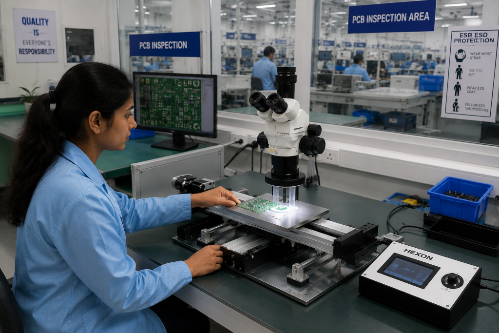
Intelligent Automation Workflow
From automated scanning to full traceability, our Automated Optical Inspection (AOI) system executes a flawless inspection workflow that reduces manual errors and increases throughput by 5x.
01
Automated Scanning
Programmable motorized XY stage supporting large-area scanning up to 300mm wafers with sub-micron repeatability. Customizable scanning paths eliminate manual positioning errors.
02
Intelligent Detection
03
Instant Classification
04
Full Traceability


Compliance & Certifications
Meets CFR 21 Part 11 Requirements For Electronic Records And Audit Trails
Ensures Data Integrity For Pharmaceutical R&D, Regulated Labs, And Quality-Controlled Production
Time-Stamps And Logs Every Parameter, Error Event, And Status Change
Complete Audit Trails Extractable For Regulatory Submission